
Separate analog bandwidth from sampling rate
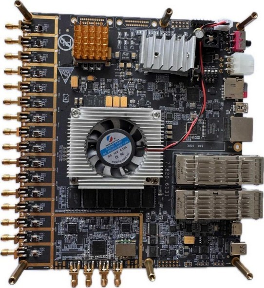
Sampling rate, input bandwidth and usable instantaneous bandwidth are related but different specifications. Start with the signal center frequency and occupied bandwidth, then check the analog input path and the planned sampling or conversion strategy. Do not infer a usable band directly from the ADC sample rate. Confirm the input filtering, frequency response and alias-management requirements with the board supplier. The HPORTEK SYHS-8R8T-2G is described as an eight-receive, eight-transmit RFSoC board with up to 2 GHz instantaneous bandwidth per channel; the exact signal path and configuration still need to be agreed for an integration project.
Build a data-rate budget before choosing the host link
An initial raw-data estimate is channel count multiplied by samples per second multiplied by bits per sample. Four channels at 1 GS/s and 16 bits per sample represent 64 Gbit/s, or 8 GB/s, before framing and transport overhead. This is an illustrative calculation, not a throughput claim for a listed product. Real systems may use container widths larger than the converter resolution, and I/Q data can change the channel accounting. Include protocol overhead, host memory bandwidth, buffering and sustained storage speed. Decide whether filtering, decimation or feature extraction must take place on the FPGA before transfer.
Distinguish converter resolution from effective performance
Nominal ADC bit depth describes the converter format; it does not by itself establish the effective resolution under every input condition. Review available noise, distortion and effective-resolution data together with their test frequency and clock conditions. Check the allowed input power and impedance for the exact channel configuration. Confirm how clipping, gain changes and invalid data are reported to software. If a required figure is absent from the public table, ask for the appropriate configuration-specific evidence rather than assuming the value from a converter component headline.
Plan the reference clock and trigger as part of the system
For coherent measurements, define which device provides the reference clock, how it is distributed and how channels are aligned. A common frequency reference alone does not guarantee sample-aligned starts or a known phase relationship. Specify trigger levels, timing, reset behavior and the required alignment after power cycling or reconnecting a link. The catalogue describes external reference and trigger support on several boards, including multi-board operation on selected models. Ask engineering to confirm the supported topology and the initialization sequence for the chosen board revision.
Confirm the FPGA processing and software boundary
List the processing that must run on the board and the work assigned to the host application. Digital down-conversion, filtering, decimation and real-time formatting can reduce transfer demand, but each function requires an implemented and supported data path. Confirm available firmware, driver support, operating systems, API documentation and example capture software. Agree on the data format, timestamp interpretation, buffer behavior and error reporting. For optical or PCIe connections, verify sustained application-level throughput rather than using the interface line rate as the final performance figure.
Use an integration checklist for a realistic acceptance test
Send channel count, center frequency, bandwidth, sample rate, acquisition duration, trigger needs, latency constraints and processing requirements to engineering. Include the host platform, available interfaces, environmental conditions and cooling plan. A practical acceptance test captures a known input, checks channel identity and time alignment, monitors dropped data, and runs for the required duration. Record firmware and software versions with the results. Public datasheets support initial comparison; they do not replace a complete integration specification or a measured system acceptance record.
Related products
- SYHS-RFSOC-PCIE · High-Speed Acquisition & Replay Card
- SYHS-8R8T-2G · Wideband RF Transceiver Board
- SYHS-16CH-S · 16-Channel Synchronous Acquisition Card
- SYHS-8CH-DRF · 8-Channel Direct RF Sampling Board
Engineering guidance for initial selection. Model-specific limits and configurations must be confirmed with HPORTEK. Calculation examples are illustrative and do not represent measured product results.
Download application note (PDF · English) ↓
Back to company updates